MOSFET Basic Overview
MOSFET comprises two abbreviations: MOS (Metal Oxide Semiconductor) + FET (Field Effect Transistor). That is, a field effect transistor that controls the switch of the semiconductor (S) conductive channel by applying voltage to the gate of the metal layer (M-metal aluminum) and the source through the oxide layer (O-insulating layer SiO2) to generate an electric field effect. Since a SiO2 insulating layer isolates the gate, source, and drain, MOSFET is also called an insulated gate field effect transistor.
The power field effect transistor that everyone refers to on the market usually refers to the insulated gate MOS type (Metal Oxide Semiconductor FET), referred to as power MOSFET (Power MOSFET). Field effect transistors are divided into two different structures: junction type and insulated gate. A field-effect transistor is a semiconductor device that uses the electric field effect of the input loop to control the output loop current. It conducts electricity only by the majority of carriers in the semiconductor and is also called a unipolar transistor.
Junction power field effect transistors are generally called static induction transistors (Static Induction Transistor-SIT). Its characteristics are that the gate voltage is used to control the drain current, the driving circuit is simple, the required driving power is small, the switching speed is fast, the operating frequency is high, and the thermal stability is better than GTR, but its current capacity is small and the withstand voltage is low. It is generally only suitable for power electronic devices with a power not exceeding 10kW.
MOSFET power field effect transistors are mostly used as switches and drivers, working in the switching state, with a withstand voltage ranging from tens of volts to thousands of volts, and an operating current of several amperes to tens of amperes. Power MOSFETs are basically enhancement MOSFET, which have excellent switching characteristics.
Classification of MOSFET
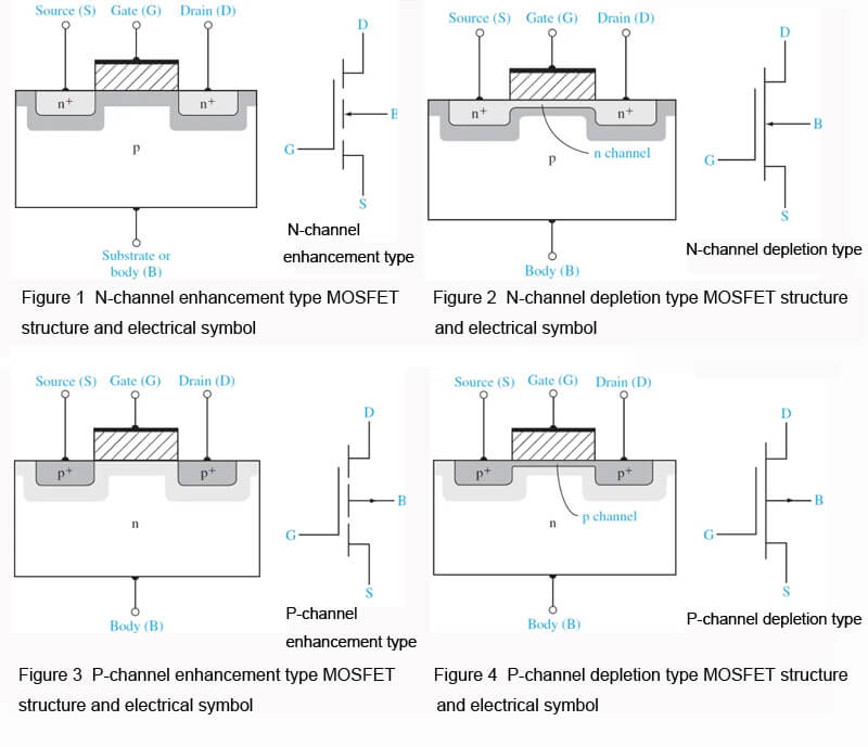
Types of MOSFET: According to the
conductive channel type, it can be divided into the
P channel and the
N channel. According to the
gate voltage amplitude, it can be divided into:
depletion type - when the gate voltage is
zero, there is a
conductive channel between the drain and source;
enhancement type - for
N (P) channel devices, a
conductive channel exists only when the gate voltage is
greater than (less than) zero. Power MOSFET is mainly an
N-channel enhancement type.
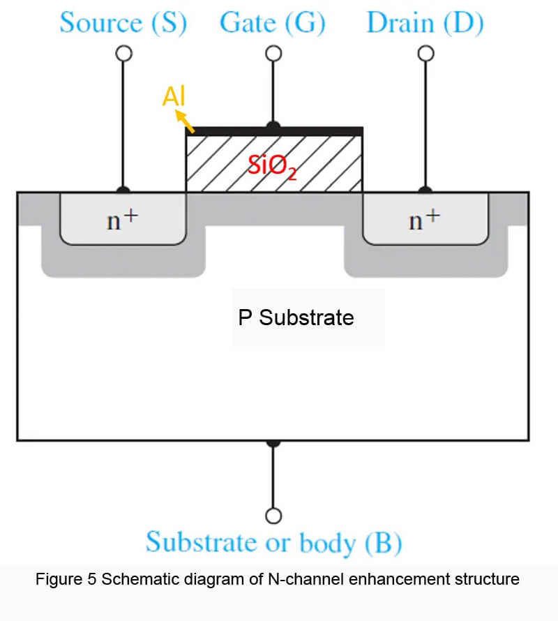
MOS tube structure principle diagram
(Take N-channel enhancement type as an example)
The structure of the N-channel enhancement MOS tube is shown in Figure 5. It uses a
low-doped P-type silicon wafer as the
substrate, uses the
diffusion process to make
two highly doped N+ regions, and introduces two electrodes, namely the
source S (Source) and the
drain D (Drain). A layer of
SiO2 insulating layer is made on the semiconductor, and then a layer of
metal aluminum Al is made on the SiO2, and the electrode is led out as the
gate G (Gate). The substrate and the source are usually connected for use. In this way, the gate and the substrate are each equivalent to a plate, with an insulating layer in the middle to form a capacitor. When the
gate-source voltage changes, the amount of
induced charge on the substrate near the insulating layer will
change, thereby controlling the size of the
drain current.
Detailed explanation of the working principle of MOS tube
(Take the N-channel enhancement type as an example)
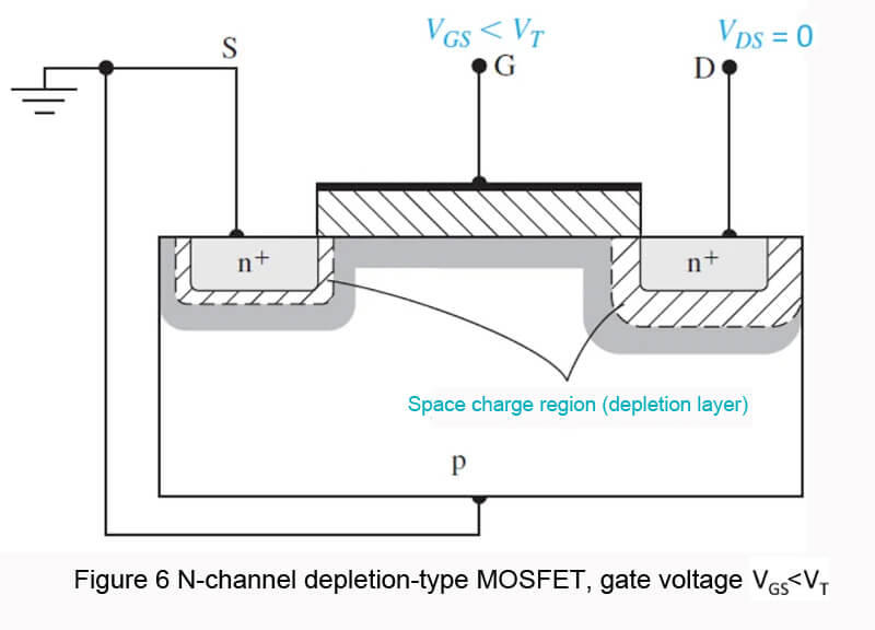
● When no voltage is applied between the gate and the source, that is, when V(GS)=0, two PN junctions are facing each other between the source and the drain. Regardless of the polarity of V(DS), there is always one PN junction that is reverse-biased, so there is no conductive channel.
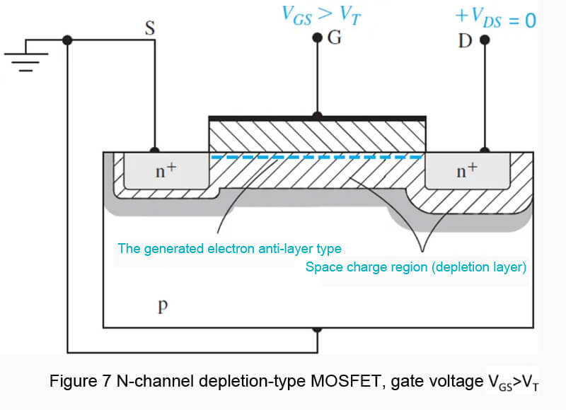
● When U(DS)=0 and U(GS)>0, the gate current is zero due to the presence of SiO2. However, the gate metal layer will gather positive charges. They repel the holes on the side of the P-type substrate close to SiO2, leaving an immobile negative ion region, forming a depletion layer, as shown in Figure 6.
● When
U(GS) increases, on the one hand, the
depletion layer widens, and on the other hand, the
free electrons of the substrate are attracted
between the
depletion layer and the
insulating layer to form a thin
N-type layer, called the
inversion layer, as shown in Figure 7. This inversion layer constitutes a conductive channel between the drain and the source. The gate-source voltage that just forms the channel is called the turn-on voltage U(GS)(th)/V(T).
The larger the U(GS) voltage,
the thicker the inversion layer formed and
the smaller the conductive channel
resistance.
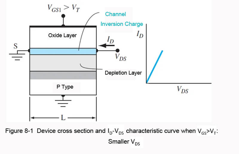
● When
V(GS)>V(T) and V(DS) is small, the schematic diagram of the basic MOS structure is shown in Figure 8-1. The thickness of the inversion channel layer in the figure qualitatively indicates the
relative charge density, which is
a constant in the channel length direction. The corresponding I(D)-V(DS) characteristic curve is shown in Figure 8-1.
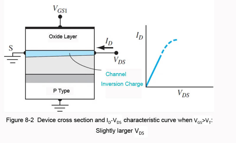
● When
V(GS)>V(T) and V(DS) increases,
the voltage drop of the oxide layer near the
drain end decreases due to the
increase of the drain voltage, which means that the
charge density of the inversion layer near the
drain end will also decrease. The channel conductance at the drain end decreases, so the slope of the I(D)-V(DS) characteristic
curve decreases, as shown in Figure 8-2.
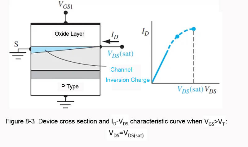
● When
V(GS)>V(T) and V(DS) increases to the point where
the oxide layer voltage drop at the drain is equal to V(T), the
charge density of the inversion layer at the drain
is zero. At this time, the
conductivity at the
drain is zero, which means that the slope of the I(D)-V(DS) characteristic
curve is zero, called
pre-pinch-off, as shown in Figure 8-3.
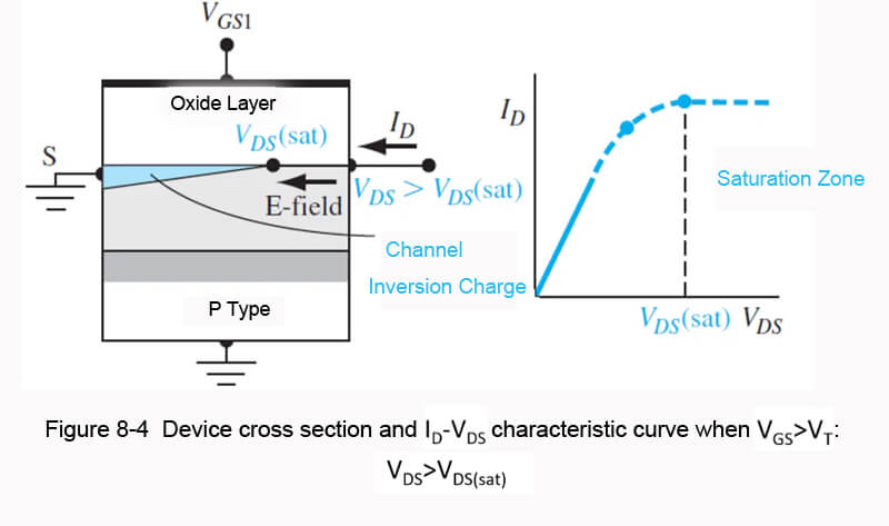
● When
V(GS)>V(T) and V(DS)>V(DS)(sat), the point in the channel where the inversion charge is zero moves toward the source end. If U(DS) continues to
increase, the pinch-off region will be
extended, as shown in the figure. The
increased part of U(DS) is almost entirely used to
overcome the
resistance of the pinch-off region to
the drain current, and the drain current
I(D) is constant. In this case, I(D)-V(DS) corresponds to the
saturation region (constant current region), as shown in Figure 8-4.
MOSFET Characteristic Curve
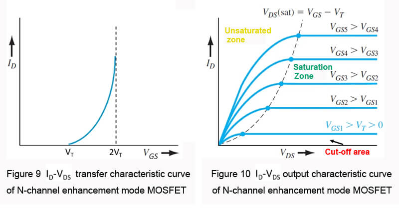
The relationship between drain current I(D) and gate-source voltage U(GS) is called the transfer characteristic of MOSFET. When I(D) is large, the relationship between I(D) and U(GS) is approximately linear, and the slope of the curve is defined as transconductance Gfs. In the figure, as V(GS) increases, the slope of I(D) increases. The reason is that as V(GS) increases, the thicker the inversion layer is formed, the smaller the on-channel resistance is, and the faster the growth rate of I(D) is.
MOSFET has three working regions:
cut-off,
saturation, and
unsaturation regions; the corresponding output characteristic curve is shown in Figure 10. If the power MOSFET works in a
switching state, that is, it
transforms back and forth between the
cut-off region and the
unsaturation region.
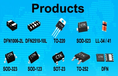
 CTK
CTK is one of the indispensable manufacturers in the
electronic manufacturing supply chain. And is one of the
mosfet manufacturers.
Such as
TO-220 Plastic Package Middle Voltage Mos. Please contact us to get free samples.