• Manufacturing test ideally would check every node in the circuit to prove it is operational.
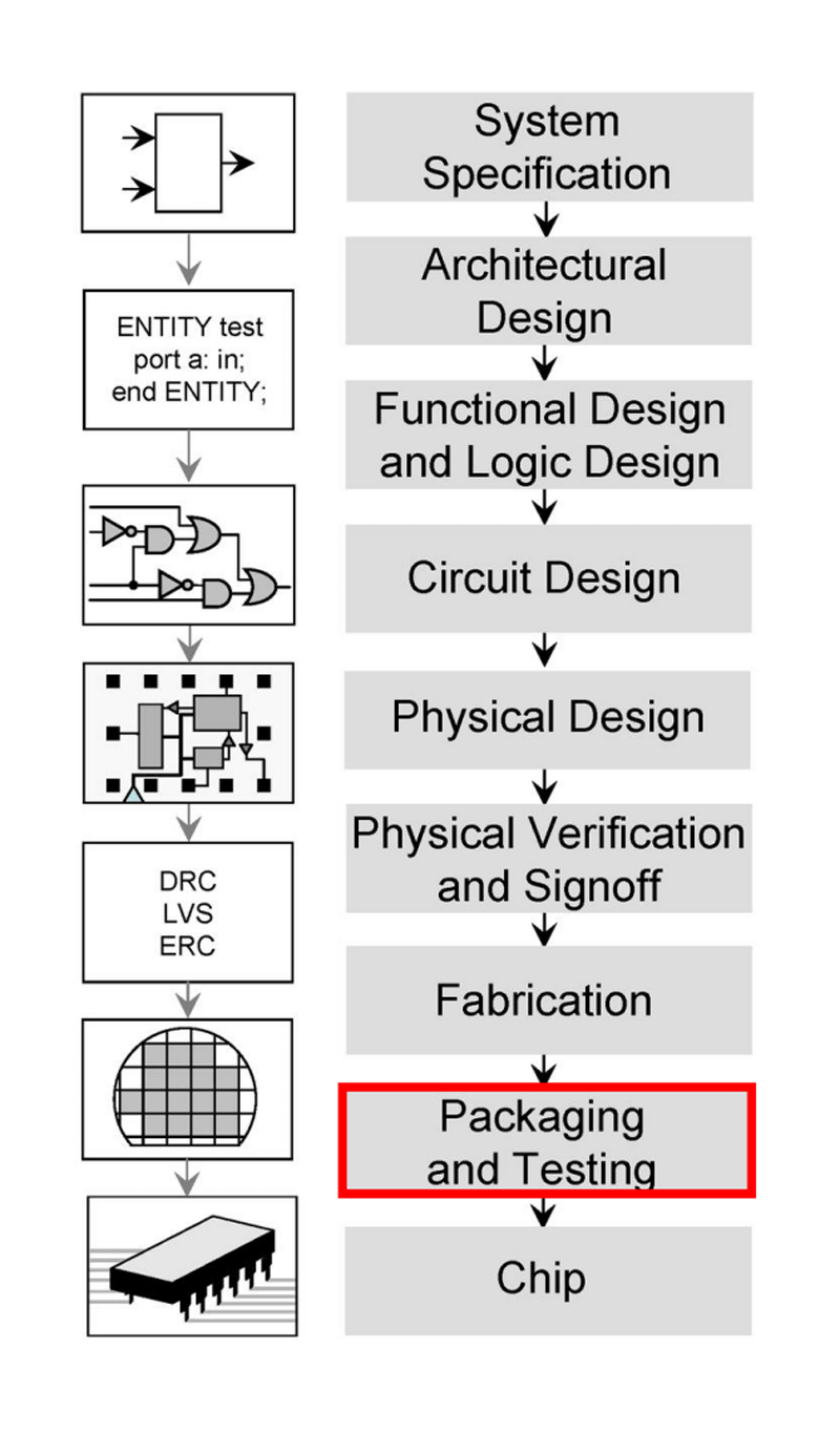
Production Test Flow
• Wafer-level testing (Wafer Sort)
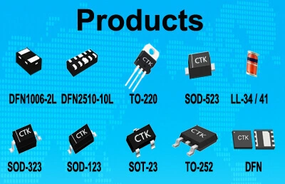
• Assembly & Packaging
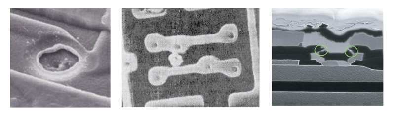
• Open/Short test
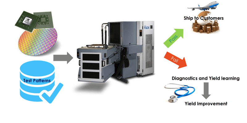
• Packaged device test
• Burn-In (@ elevated voltage and temperature)
• Final Test (pass/fail) and Bin Sorting
• Parametric Tests (voltage, temperature, and clock)
• Shmoo plot
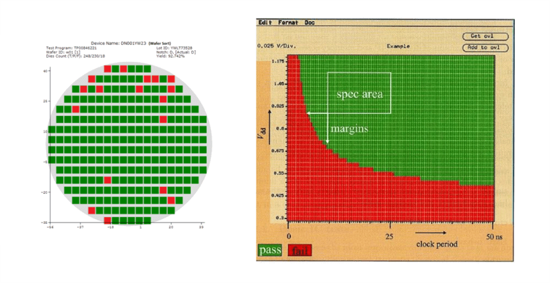
Wafer Sort
• Wafer sort or probe test
• Done before wafer is scribed and cut into chips
• Includes test site characterization – specific test devices are checked with specific patterns to measure gate threshold, poly sheet resistance, etc.
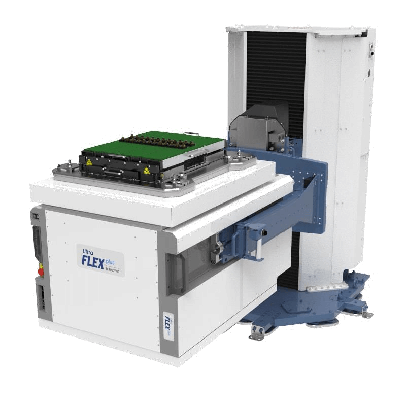
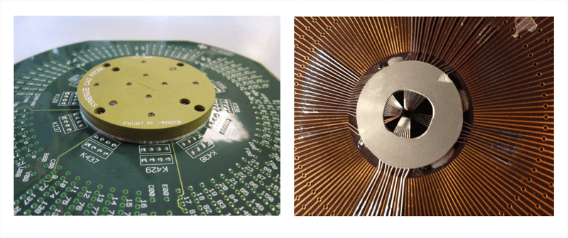
• Probe card
• Custom built PCB to allow performing wafer sort
• Modern probe cards can test an entire 12" wafer with one touchdown
• Can contact several dies in parallel (~1-16)
• Camera in the wafer prober allows alignment
Electrical Testing
• DC Parametric Tests
• DC contact test - Calculates pin resistance
• Power consumption test - Measure max current at worst case temperature
• Output short circuit test - Measure current driven when output short circuited
• Output drive current test - Measure current for ‘1’ and ‘0’ outputs
• Threshold test - Measure VIH, VIL of input pads
• AC Parametric Tests
• Rise/Fall time tests
• Setup/Hold time tests
• Propagation delay tests
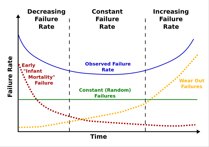
Burn-in or Stress Test
• Process:
• Subject chips to high temperatures and over-voltage supply, while running production tests
• For example: 125C for 168 hours
• Catches:
• Infant mortality cases – these are damaged or weak (low reliability) chips that will fail in the first few days of operation – burn-in causes bad devices to fail before they are shipped to customers
• Freak failures – devices having the same failure mechanisms as reliable devices