Application Characteristics
SiC MOSFETs offer superior switching performance and higher thermal conductivity, enabling more compact and efficient power systems in EVs, solar inverters, and industrial drives.


1. The on-state resistance changes little with temperature, and the on-state impedance remains low at high temperatures, allowing it to operate well in harsh environments.
2. As the gate voltage increases, the on-state resistance becomes smaller, showing behavior closer to a voltage-controlled resistor. Turn-on requires relatively small gate charge, and overall driving power is low. Its body diode has a higher Vf, but very good reverse recovery characteristics, which can reduce turn-on losses.
3. It has smaller junction capacitance, faster turn-off speed, and lower turn-off loss.
4. Switching loss is small, enabling high-frequency switching operation, which allows passive components such as filters to be miniaturized and improves power density.
5. The turn-on voltage is higher than that of Si devices. It is recommended to use Vgs of 15V, 18V, or 20V. Although the threshold voltage is only 2.7V, full turn-on can only be achieved when the gate drive voltage reaches 15V to 20V.
6. It has slightly poorer resistance to false triggering. When used in bridge circuits, an active clamping circuit or negative voltage should be applied to prevent false triggering.
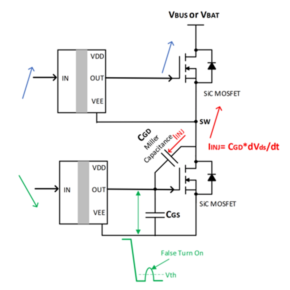
High dv/dt causes false turn-on of SiC MOSFET
SiC MOSFETs offer superior switching performance and higher thermal conductivity, enabling more compact and efficient power systems in EVs, solar inverters, and industrial drives.
1. The trigger pulse should have a relatively fast rise and fall time, with steep edges.
2. The impedance of the drive circuit should be low, enabling rapid gate charging and discharging.
3. The drive circuit must provide sufficiently large drive current.
4. A sufficiently high gate voltage is required to minimize conduction losses.
5. Use of a negative voltage for turn-off is recommended to prevent false triggering.
6. Parasitic inductance in the gate loop should be minimized.
7. The peak drive current (Imax) should be large to reduce the Miller plateau duration.
| Parameter | Si MOSFET | Si IGBT | SiC |
|---|---|---|---|
| Switching Frequency | High (>20 kHz) | Medium/Low (5 kHz - 20 kHz) | High (>50 kHz) |
| Basic Protection | None | Desaturation protection, Miller clamp | Current sensing, Miller clamp |
| VDD Maximum Rating | 20 V | 30 V | 30 V |
| VDD Clamping | 0 - 20 V | 10 - 20 V | -5 to 25 V |
| Operating VDD | 10 - 12 V | 12 - 15 V | 15 - 18 V |
| UVLO (Undervoltage Lockout) | 8 V | 12 V | 12 - 15 V |
| CMTI (Common Mode Transient Immunity) | 50 - 100 V/ns | < 50 V/ns (less critical) | > 100 V/ns |
| Propagation Delay | The lower, the better (<50 ns) | Not critical | The lower, the better (<50 ns) |
| Power Rail Voltage | Up to 650 V | > 650 V | > 650 V |
| Typical Applications | Power supplies (servers, telecom), EV OBC, solar inverters (<3 kW) | Motor drives, UPS, solar inverters (>3 kW), traction inverters | PFC, PV inverters, EV DC/DC, rail, high-end drives |
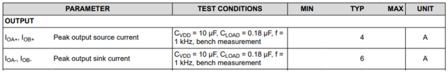
Figure 2: SiC MOSFET Front View
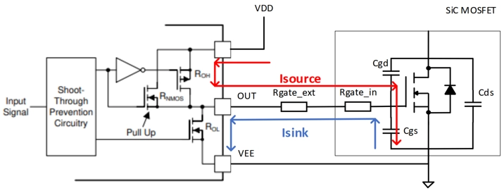
Figure 3: SiC MOSFET Back View
Driver ICs generally control the switching of MOSFETs or IGBTs by sourcing current (source current) and sinking current (sink current) to charge and discharge the gate capacitance. To realize the fast switching characteristics of SiC MOSFETs, achieving lower switching losses and higher switching frequencies, larger drive current is usually required. The datasheet of the driver chip usually specifies the maximum sourcing and sinking current capabilities it can withstand.
As shown in Figure 2, the peak sourcing and sinking current values of the TI dual-channel isolated gate driver UCC21530 are described. In general, this corresponds to the saturation current of the output-stage MOSFETs in the driver chip. However, in practical systems, the maximum current is often related to parameters such as the supply voltage, gate resistance, and parasitic components in the gate drive loop.
Figure 3 shows the charging and discharging paths of the gate capacitance in the gate drive loop during the switching process.
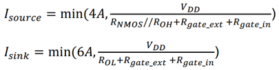
Figure 4
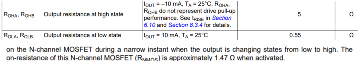
Figure 5:Driver Output Resistance Description in the UCC21530-Q1 Datasheet
In actual driving conditions, the peak values of the source and sink current are often limited by the impedance of the gate drive loop. This includes not only the internal pull-up and pull-down resistances (ROL, ROH) of the driver IC, but also the external gate resistance (Rgate_ext) and the internal gate resistance of the MOSFET (Rgate_in).
Taking the UCC21530 as an example, the actual maximum turn-on and turn-off drive currents of the chip are shown in Figure 5.The values of ROL, ROH, and RNMOS are generally provided in the datasheets of the driver ICs.
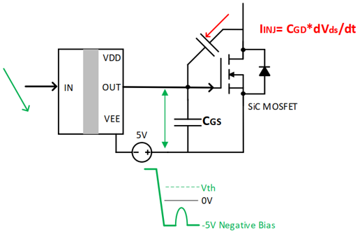
Negative gate drive prevents false turn-on.
To avoid the risk of shoot-through during switching transitions, SiC MOSFETs typically require negative gate drive. By applying a negative voltage during turn-off, it ensures that even if small voltage spikes occur, the gate voltage will not exceed the threshold voltage and unintentionally turn the MOSFET on.
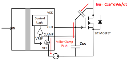
Figure 6: Driver ICs with integrated Miller clamping prevent MOSFET false turn-on.
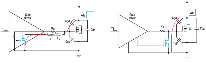
Figure 7/8: Gate driver with integrated Miller clamping/Gate driver with external Miller clamping
Another common method to prevent false turn-on of SiC MOSFETs is to implement a Miller clamping circuit or use a chip with a Miller clamping function, as shown in Figure 6. The Miller clamping function works by sampling the gate voltage and comparing it with the threshold voltage. When the gate voltage drops below the threshold voltage, the comparator flips, causing the built-in Miller clamping MOSFET to turn on. This creates a low impedance path, which effectively clamps the gate of the SiC MOSFET and prevents false turn-on The position of the Miller clamp greatly affects its effectiveness.
The purpose of clamping is to provide a low impedance path for the Miller current to flow towards the ground. Using an internal clamp reduces the components needed for circuit construction, and the clamp should be placed as close as possible to the power switch. The Miller current path may include parasitic resistance (Rp) and inductance (Lp), as shown in Figure 7. If the current is large enough, the Miller clamp will not significantly affect the performance of the driver. An external Miller clamp is controlled by the driver and is placed externally, as shown in Figure 8. This configuration allows the clamp to be positioned very close to the power switch to minimize any impedance in the current path..
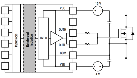
Figure 9: UVLO Referencing COM Pin
SiC MOSFETs feature high power density and typically require higher drive voltages to fully turn on. This ensures minimal on-resistance, lowest conduction losses, and maximum current delivery capability. The under-voltage lockout (UVLO) of the driver IC defines the minimum drive voltage at which the switch can function correctly. To prevent false turn-on of the SiC MOSFET, a negative voltage supply is usually employed for gate drive. It’s important to note that for most driver ICs without a dedicated COM pin, the UVLO typically references the IC’s VEE/VSS pin. As an example, consider the SiC MOSFET A3M018F120QAN, with a typical turn-on threshold of Vth = 2.8V. In a system with a negative gate drive of -4V, if an 8V UVLO driver IC is used, the actual minimum Vgs for the SiC MOSFET to operate would be 8V - 4V = 4V, which is just slightly above the MOSFET’s turn-on threshold. Under such conditions, the on-state resistance increases from 16mΩ (fully on) to an Ω-level.
This demonstrates that when the gate drive voltage is insufficient, the on-resistance increases rapidly, potentially causing the system to overheat quickly. This can negatively affect both the long-term reliability of the MOSFET and the overall safety of the system. For this reason, it is generally recommended to choose a driver IC with a UVLO threshold of 12V.
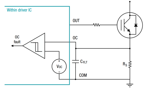
Figure 10: Overcurrent in FETs with Integrated Current Regulation Function
DESAT is a common short-circuit protection method for IGBTs. However, due to differences in I-V characteristics, it is not always suitable for SiC MOSFETs. The transition of a SiC MOSFET from the linear region to the saturation region is not clearly defined, so using a single voltage threshold for DESAT detection may not be very accurate. A more applicable method is overcurrent detection, which measures the current flowing through a precision shunt resistor (Rshunt). Although Rshunt is typically in the milliohm range and carries relatively large currents—resulting in higher power losses—it offers more accurate monitoring with fewer required circuit components. Fewer components mean faster response time, which is critical for SiC MOSFETs due to their shorter short-circuit withstand time (SCWT) compared to IGBTs.
To address the power loss issue, some power modules integrate current scaling functions to reduce the current flowing through the shunt resistor (see Figure 10). The built-in shunt circuit within the module reduces the power dissipated across the shunt resistor. The corresponding scaling ratio is provided by the power device manufacturer. This approach results in lower power consumption than traditional shunt-based measurements and enables more accurate current sensing
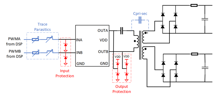
Figure 11: Building an Isolated Power Supply Circuit Using Dual Low-Side Drivers
To provide power to the SiC MOSFET driver through an isolated power supply, common methods include full-bridge resonant circuits, among others. The mainstream industry solution uses dual low-side drivers, such as the TI UCC27524-Q1, with two outputs directly driving a transformer to achieve isolated power supply, as shown in Figure 11.
| Part Number | VR | Current | Package | SPQ | L/T |
|---|---|---|---|---|---|
| TK3D06065F | 650V | 6A | TO-252-2L | 2500 | 1~3Weeks |
| TK3D10065F | 650V | 10A | TO-252-2L | 2500 | 1~3Weeks |
| TK3D10065E | 650V | 10A | TO-263-2L | 2500 | 1~3Weeks |
| TK3D06065N | 650V | 6A | DFN 5×6 | 3000 | 1~3Weeks |
| TK3D06065G | 650V | 6A | DFN 8×8 | 3000 | 1~3Weeks |
| TK3D10065G | 650V | 10A | DFN 8×8 | 3000 | 1~3Weeks |
| TK3D06065A | 650V | 6A | TO-220-2L | a | 1~3Weeks |
| TK3D10065A | 650V | 10A | TO-220-2L | 50 | 1~3Weeks |
| TK3D10065H | 650V | 10A | TO-247-2L | 30 | 1~3Weeks |
| TK3D15065A | 650V | 15A | TO-220-2L | 50 | 1~3Weeks |
| TK3D20065A | 650V | 20A | TO-220-2L | 50 | 1~3Weeks |
| TK3D20065H | 650V | 20A | TO-247-2L | 30 | 1~3Weeks |
| TK3D20065D | 650V | 20A | TO-247-3L | 30 | 1~3Weeks |
| TK3D30065H | 650V | 30A | TO-247-2L | 30 | 1~3Weeks |
| TK3D30065D | 650V | 30A | TO-247-3L | 30 | 1~3Weeks |
| TK3D40065H | 650V | 40A | TO-247-2L | 30 | 1~3Weeks |
| TK3D42090H | 900V | 42A | TO-247-2L | 30 | 1~3Weeks |
| TK3D02120F | 1200V | 2A | TO-252-2L | 2500 | 1~3Weeks |
| TK3D05120A | 1200V | 5A | TO-220-2L | 50 | 1~3Weeks |
| TK3D06120F | 1200V | 6A | TO-252-2L | 2500 | 1~3Weeks |
| TK3D10120A | 1200V | 10A | TO-220-2L | 50 | 1~3Weeks |
| TK3D20120A | 1200V | 20A | TO-220-2L | 50 | 1~3Weeks |
| TK3D20120H | 1200V | 20A | TO-247-2L | 30 | 1~3Weeks |
| TK3D20120D | 1200V | 20A | TO-247-3L | 30 | 1~3Weeks |
| TK3D30120H | 1200V | 30A | TO-247-2L | 30 | 1~3Weeks |
| TK3D30120D | 1200V | 30A | TO-247-3L | 30 | 1~3Weeks |
| TK3D40120H | 1200V | 40A | TO-247-2L | 30 | 1~3Weeks |
| TK3D40120D | 1200V | 40A | TO-247-3L | 30 | 1~3Weeks |
| TK3D50120H | 1200V | 50A | TO-247-2L | 30 | 1~3Weeks |
| TK3M30065K | 650V | 30mΩ | TO-247-4L | 30 | 4~12Weeks |
| TK3M60065K | 650V | 60mΩ | TO-247-4L | 30 | 4~12Weeks |
| TK3M25075K | 750V | 25mΩ | TO-247-4L | 30 | 1~3Weeks |
| TK3M55075M | 750V | 55mΩ | TO-263-7L | 30 | 1~3Weeks |
| TK3M55075K | 750V | 55mΩ | TO-247-4L | 30 | 1~3Weeks |
| TK3M14120K | 1200V | 14mΩ | TO-247-4L | 30 | 4~12Weeks |
| TK3M30120K | 1200V | 30mΩ | TO-247-4L | 30 | 1~3Weeks |
| TK3M30120M | 1200V | 30mΩ | TO-263-7L | 30 | 1~3Weeks |
| TK3M35120D | 1200V | 35mΩ | TO-247-3L | 30 | 1~3Weeks |
| TK3M35120M | 1200V | 35mΩ | TO-263-7L | 30 | 1~3Weeks |
| TK3M40120K | 1200V | 40mΩ | TO-247-4L | 30 | 4~12Weeks |
| TK3M40120D | 1200V | 40mΩ | TO-247-3L | 30 | 1~3Weeks |
| TK3M50120K | 1200V | 50mΩ | TO-247-4L | 30 | 4~12Weeks |
| TK3M68120M | 1200V | 68mΩ | TO-263-7L | 30 | 1~3Weeks |
| TK3M80120K | 1200V | 80mΩ | TO-247-4L | 30 | 4~12Weeks |
| TK3M80120M | 1200V | 80mΩ | TO-263-7L | 30 | 1~3Weeks |
| TK3M160120E | 1200V | 160mΩ | TO-263-2L | 2500 | 4~12Weeks |
| TK3M160120D | 1200V | 160mΩ | TO-247-3L | 30 | 4~12Weeks |
| TK3M160120K | 1200V | 160mΩ | TO-247-4L | 30 | 4~8Weeks |
| TK3M45170D | 1700V | 45mΩ | TO-247-3L | 30 | 4~8Weeks |
| TK3M10017D | 1700V | 1Ω | TO-247-3L | 30 | 4~8Weeks |
Through this comprehensive overview, we have explored the key characteristics, application advantages, and essential gate driver requirements of SiC MOSFETs. By understanding driver current sourcing/sinking, negative gate drive techniques, Miller clamping methods, UVLO behavior, and overcurrent protection, engineers can optimize their power system designs for higher efficiency, reliability, and robustness. These insights also help in selecting the right isolated power supply architecture and device packaging for various application needs.
CTK is a semiconductor manufacturer dedicated to delivering high-performance SiC MOSFET solutions for applications including electric vehicles, renewable energy systems, energy storage, industrial drives, and aerospace. We are committed to enabling next-generation power conversion with cutting-edge device technology and reliable production capabilities.


We use cookies to enable our website to function properly, to personalize content and ads, to provide social media features, and to analyze traffic.