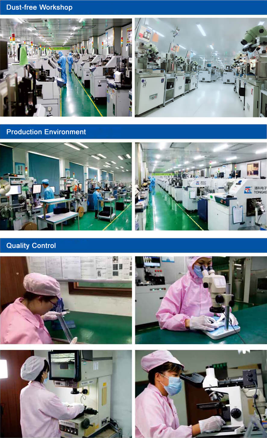
PRODUCTION SITE
Our workshops are
dust-free workshops,
Clean Room Class: 10000
The entire industry chain: Continuous cost optimization capabilities under quality assurance.
1. Chip design: Customized design service, specially hired Chinese Academy of Sciences academicians, PhD research and development team, and well-known universities for industry-university-research cooperation.
2. Wafer manufacturing: Wafer production capacity supply guarantee.
4. Sales channel: Marketing dual-channel service guarantee, factory direct sales, and face-to-face docking service for major customers.
5. Terminal manufacturers: Industry TOP cooperation experience (TCL, FOXCONN, ZTE, MI, JBL, TenPao, AVC).
Complete product line:
Our products cover a wide range from small signal discrete devices to power devices, from micro-chip DFN/QFN packaging to TO series packaging
 ESD PROCESS INTRODUCTION
We have our own package line: guaranteed quality, guaranteed quantity, and fast delivery.
Production Process: Wafer cutting  Die Bonding
 Wire bonding
 Injection molding
 Electroplate
 Punching
 Testing&Taping
  Quality Checking and Warehousing
Engineering Experiment Center Reliability Testing and Failure Analysis:
CTK Laboratory can complete all experimental projects and has comprehensive failure analysis capabilities


