• The diode consists of two types of semiconductor materials:
• P-type region: Contains positively charged "holes" as the majority carriers, created by doping with elements like boron.
• N-type region: Contains negatively charged free electrons as the majority carriers, introduced by doping with elements like phosphorus.
• At the interface of these two regions, a p-n junction forms. This junction is the key functional area of the diode.
• At the p-n junction, electrons and holes recombine, creating a depletion region.
• This region is free of mobile charge carriers and generates an internal electric field that controls the flow of current.
• Anode: The positive terminal, connected to the p-type region.
• Cathode: The negative terminal, connected to the n-type region.
• These terminals allow the diode to interface with external circuits.
• The diode's semiconductor structure is enclosed in a protective casing, which can be designed for various applications:
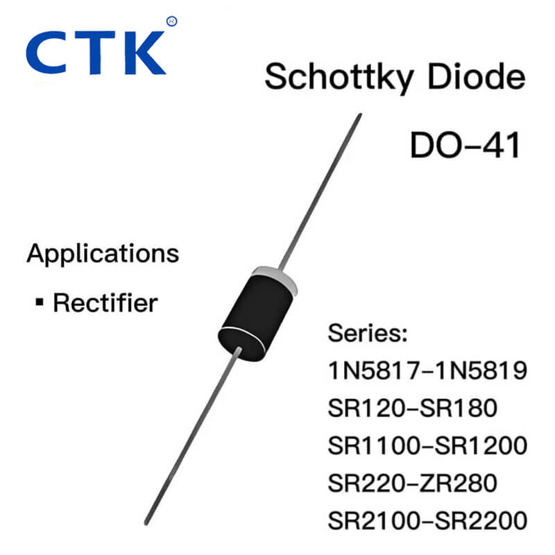
• Through-hole packages (e.g., DO-41 for general-purpose diodes).
DO-41 Schottky Diode 1N5817-1N5819
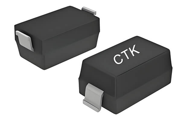
• Surface-mount packages (e.g., SOD-123 for compact electronic devices).
SOD-123 Plastic-Encapsulate Zener Diodes
• The packaging often includes polarity markings to identify the anode and cathode.
Depending on the application, diodes may have additional features or specialized structures:
• Rectifier diodes for power conversion.
• Zener diodes for voltage regulation.
• Schottky diodes for high-speed switching.
• LEDs (Light-Emitting Diodes) for illumination and indicators.
This structure enables diodes to control electrical flow, making them essential components in various electronic systems. For more information about diode products, visit CTK diodes catalog.