Overview
Semiconductor (Including
Diode,
Transistor) chip packaging is the process of placing chips and other parts on a frame. It involves connecting them and leading out the terminals.
The chips are then fixed using a plastic insulating medium through injection molding. This creates a complete three-dimensional structure using film technology and micro-processing technology. This concept is a narrow definition of packaging.
In a broader sense, packaging refers to the packaging project, which connects and fixes the package body to the substrate, assembling it into a complete system, and ensuring the comprehensive performance of the entire system. Combining the previous two definitions constitutes a broad concept of packaging.
The future of packaging will mainly be plastic packaging, and glass packaging will gradually shrink and be eliminated due to poor reliability and environmental protection issues.
The Role and Purpose of Packaging
• Protection: Semiconductor chip production workshops have very strict production condition control, constant temperature (230±3℃), constant humidity (50±10%), strict air dust particle size control (generally between 1K and 10K), and strict electrostatic protection measures. The exposed chip will not fail only under such strict environmental control.
However, the surrounding environment we live in is completely impossible to have such conditions. The low temperature may be -40℃, the high temperature may be 60℃, and the humidity may reach 100%. Its operating temperature may be as high as 120℃ or above if it is an automotive product. To protect the chip, we need packaging.
• Support: The support has two functions. One is to support the chip and fix the chip to facilitate the connection of the circuit. The other is to form a certain shape after the packaging is completed to support the entire device and make the entire device less prone to damage.
• Connection: The function of the connection is to connect the electrode of the chip with the external circuit. The pin is used to connect with the external circuit, and the gold wire or copper wire connects the pin and the chip circuit. The frame Pad is used to carry the chip, the epoxy resin adhesive is used to stick the chip on the frame Pad, the pin is used to support the entire device and in the circuit board, and the plastic package plays a fixing and protective role.
• Reliability: Any package needs to form a certain reliability, which is the most important measurement indicator in the entire packaging process. The original chip will be damaged after leaving the specific living environment and needs to be packaged. The working life of the chip is mainly determined by the choice of packaging materials and packaging processes, while the electrical parameters are determined by the core chip.
Form of Packaging
According to the connection method with the PCB, it is divided into:
• Plug-in packaging: PTH-Pin Through Hole, through-hole (plug-in) type;
• SMD packaging: SMT-Surface Mount Technology, surface mount type. At present, most diodes/transistors on the market are SMT type.
According to the packaging material, it is divided into:
• Metal packaging: mainly used in military or aerospace technology, no commercial products;
• Ceramic packaging: better than metal packaging, also used in military products, occupying a small commercial market;
• Glass and plastic packaging: used in consumer electronics, because of its low cost, simple process, high reliability, and occupying the vast majority of the market share.
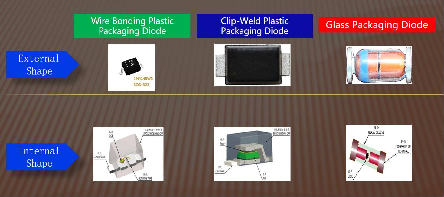
Packaging form comparison

Raw materials for packaging
1. Wafer
Wafer refers to the silicon wafer used in the production of silicon semiconductors. Because of its round shape, it is called a wafer; various circuit component structures can be processed on the silicon wafer to become a semiconductor product with specific electrical functions.
2. Lead Frame (L/F)
• Provides circuit connection and fixation of Die;
• Main materials are copper and iron-nickel alloy, and silver plating, NiPdAu, and other materials will be performed on it;
• L/F has two processes: Etch corrosion and Stamp engraving;
• Easy to oxidize, stored in a nitrogen cabinet with humidity less than 40%RH;
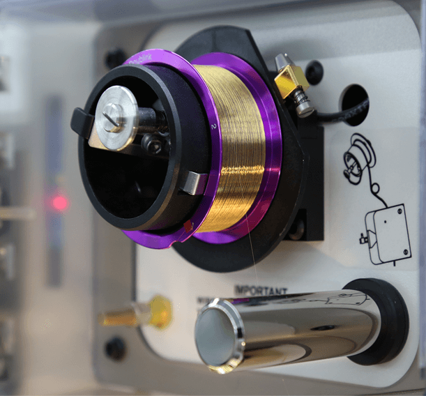
3. Bonding Wire
• Realize electrical and physical connection between the chip and external lead frame;
• Gold wire uses 99.99% high-purity gold;
• At the same time, for cost considerations, copper wire and aluminum wire processes are currently used. The advantage is that the cost is reduced, while the process difficulty is increased and the yield is reduced;
• The wire diameter determines the current that can be conducted: usually, there are wire diameters such as 0.8mil, 1.0mil, 1.2mil, 1.5mil, and 2.0mil;
• Easy to oxidize, stored in a nitrogen cabinet with humidity less than 40%RH.
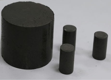
4. Mold Compound
• Main ingredients: epoxy resin and various additives (curing agent, modifier, mold release agent, dye, flame retardant, etc.)
• Main function: Wrap the Die and Lead Frame in a molten state to provide physical and electrical protection to prevent external interference;
• Storage conditions: Store at -5°C and return to normal temperature for 24 hours;
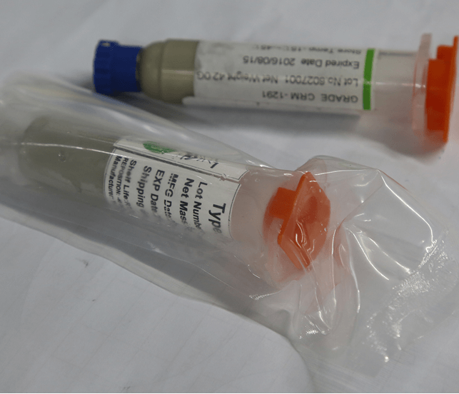
5. Silver Glue--Epoxy
• The ingredients are epoxy resin filled with metal powder (Ag);
• There are three functions: fix the Die on the Die Pad; heat dissipation, conductivity;
• Store below -15°C and return to normal temperature for 2 hours before use
